Understanding the Dynamics of Semiconductor Manufacturing: Yield Analysis and Yield Management Systems
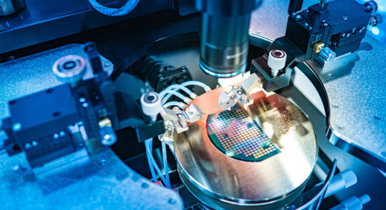
The science and art of semiconductor manufacturing, responsible for powering the digital revolution, constitute one of the most intricate, detailed, and complicated processes of the modern industrial world. The essence of this complex multistage operation lies in creating integrated circuits, miniature electronic circuits that have found their way into almost every electronic device. These electronic marvels govern our digital world, from computers and smartphones to cars and kitchen appliances, and beyond.
The manufacturing of these semiconductors is a fascinating process that involves several layers of science – physics, chemistry, and materials science – and combines them with precision engineering to create devices that are continuously shrinking in size while increasing in capabilities. This process is a testament to human ingenuity, involving billions of dollars of advanced equipment, and is growing increasingly complex due to reductions in feature size and the rising number of devices. However, amid this complexity, certain aspects stand out due to their impact on the manufacturing process: Semiconductor Yield Analysis, the Fabless Semiconductor business model, and Yield Management Systems.
Semiconductor Yield Analysis and the Impact of Spatial Defects and Radial Yield Losses
One of the most critical performance metrics in semiconductor manufacturing is the yield rate. Yield in this context refers to the ratio of correctly functioning chips to the total chips on a silicon wafer. It is an imperative element that significantly impacts the economics of semiconductor manufacturing. The higher the yield, the lower the production cost per chip, directly affecting a company’s profitability.
Yield analysis software is a systematic approach employed to identify and rectify the defects in the manufacturing process to optimize the yield. This process typically involves a detailed analysis of the production stages to determine potential problem areas and devise appropriate solutions.
A significant aspect of yield analysis is yield modeling. Yield modeling employs a combination of probabilistic models and critical factors like spatial defects and radial yield losses to anticipate potential yield. Probabilistic models offer a comprehensive view of the yield by considering a myriad of variables that can affect the yield, such as process variation, design complexity, and tool parameters.
Spatial defects refer to defect clusters in a localized region of the wafer yield in manufacturing, often due to issues with specific equipment or process steps. These defects can significantly reduce the yield, as they can render a large portion of the wafer unusable.
Radial yield loss is another critical factor that can affect the yield. This typically occurs due to edge effects, where the edge of the wafer is exposed to different conditions than the center, leading to inconsistent processing and, therefore, lower yield at the wafer’s edge.
The Fabless Semiconductor Business Model: An Overview and Impact on the Industry
The term “fabless” refers to a business model where semiconductor companies outsource the manufacturing aspect to third-party factories or foundries while focusing on the design, development, and marketing of semiconductor products.
This model allows companies to leverage the manufacturing expertise of specialized foundries, freeing them to focus on their core competencies such as product design and innovation. This model offers numerous benefits, such as cost reduction, improved flexibility in responding to market demands, and resource reallocation toward research and development.
However, the fabless model does present some challenges. These include potential quality control issues due to less direct control over manufacturing, potentially higher costs due to the intricacies of chip design and fabrication, and supplier volatility.
Yield Management Systems (YMS): Role and Impact on Semiconductor Manufacturing
Yield Management Systems (YMS) are an essential cog in the wheel of semiconductor manufacturing. They manage the data collection, analysis, and tool system from the fab, especially during the manufacturing ramp-up phase. By effectively processing and analyzing vast amounts of data, YMS can provide insightful reports that highlight potential yield-impacting issues.
YMS is used by various entities in the semiconductor ecosystem, including Integrated Device Manufacturers (IDMs), fabs, fabless semiconductor companies, and Outsourced Assembly and Test services (OSATs). With the rising complexity of semiconductors, escalating costs, and the demand for longer-lasting chips, the industry is witnessing increasing interest in YMS.
Modern YMS leverage advances in data analytics, automation, and intuitive graphical interfaces to offer comprehensive yield management solutions. Investment in YMS not only comes from established manufacturers but also startups, signaling the vital role of YMS in the semiconductor industry’s future.
Conclusion
The semiconductor manufacturing industry, a fundamental driver of the digital age, is a complex labyrinth where science and technology converge to create marvels of modern electronics. As we have journeyed through the intricate operations of this industry, it becomes clear that several crucial aspects dictate its functioning – semiconductor yield analysis, the fabless semiconductor model, and Yield Management Systems.
The yield analysis underlines the very essence of the manufacturing process – creating maximum functional chips with minimum resources. The more we can predict and manage the yield, the more efficiently we can operate, directly affecting a company’s bottom line. Simultaneously, the fabless model offers a new paradigm for companies to navigate the competitive semiconductor landscape, focusing on their strengths while leveraging the capabilities of specialized foundries.
Finally, the advent of Yield Management Systems, powered by advanced data analytics and automation, has revolutionized the way we perceive and manage yield. By understanding and implementing these systems, companies can unearth hidden patterns, pinpoint potential issues, and devise strategies to enhance yield.
References
- “Semiconductor Manufacturing: The Basic Process.” Semiconductor Manufacturing Technology, 2nd Edition. May, Gary S., and Costas J. Spanos. Wiley-IEEE Press, 2006.
- Stapper, Charles H. “Modeling of integrated circuit defect sensitivities.” IBM Journal of Research and Development 27.6 (1983): 549-557.
- “Fabless: The Transformation of the Semiconductor Industry.” Daniel Nenni and Paul McLellan, SemiWiki Project, 2014.
- Huang, Guangyong. “An effective yield management system (YMS) in semiconductor manufacturing industries.” Microelectronics Reliability 55.3-4 (2015): 523-528.